MMi203: External digital inputs
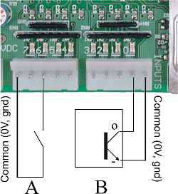
The above picture shows the two (digital) input connectors and a couple of typical input devices.
Each connector contains the connections for 4 inputs, plus a common pin that connects onboard to the power supply 0V. The common pin on each input connector is provided simply as a convenience to you when wiring to the board.
In the picture A is a simple switch connected to input 6. B is the output of an NPN style sensor connected to input 0. The sensor would also require a positive supply voltage to power it. See the manufacturer's data for connection details of the sensor you are using. The terminal labeled with a minus sign above will be the manufacturer's designated negative or common terminal, and the "O" terminal will be the designated output terminal of the sensor.
The input is ON when the input pin is connected to 0V (Gnd). Under that condition a (positive) current flows out of the input pin, through the external circuit, to 0V. The magnitude of that current depends on the supply voltage. Assuming a dead short between the input pin and 0V, the current is given by the equation
I(in) = - (V(supply) - 2V) / 10000
The leading minus sign simply means the current is flowing out of the pin. The 2V represents the voltage drop of the input indicator LED. The 10000 represents the 10K input pullup resistance.
This equation translates to about 1mA with a 12V supply and 2.2mA with a 24V supply. This is low enough to be compatible with all off-the-shelf NPN style sensors. The inputs are not compatible with PNP style sensors.
Take care when driving the inputs from switch or relay contacts. The problem is "contact wetting" (or a lack of it) and due not to too much current but to too little current. You should select contacts that are designed for low level switching. There is an article about this here.
You should also be aware that the board will only recognise the input as ON when the voltage on the input pin is typically less than 2.3V (1.5V worst case). That means the input needs to be a "fairly solid" connection to 0V.
A word of caution: In practice the threshold voltage of the input, as defined by the processor chip, is approximately 2.3V or a little less. However, the chip manufacturer (Motorola) only guarantees that an input will be treated as low (in our case ON), if the voltage is below 1.5V. Similarly, the chip is guaranteed to treat as high (OFF) only voltages above 3.5V. The range between 1.5V and 3.5V is a "no man's land" where behaviour is not guaranteed. That means that you may determine experimentally that something works OK on a prototype, but that gives you no right to assume it will therefore work on all future units.
Note that the threshold voltage varies from product to product. Don't assume that what applies to this board will apply to others.
The external inputs have a built in hardware noise filter for improved compliance with electromagnetic emission requirements. The input filter introduces a delay in the input response time. The delay times are different for OFF and ON, and vary with the supply voltage. Turn-on time is less than 1µS. Turn-off time is approximately 500µS divided by the supply voltage, i.e. 42µS at 12V and 21µS at 24V.
How to blow up the inputs
You can blow up the inputs by:
- Applying a positive voltage 5V above the positive supply. This can damage the indicator LED instantaneously by reverse voltage breakdown;
- Applying a negative voltage of more than (32V - The positive supply voltage). This will damage the input pullup resistors due to overheating. This is not a sudden death failure. The pullup resistors are rated at 200mW.