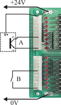
The picture above shows the two I/O connectors and two typical input devices.
Each connector contains the connections for 8 I/Os.
In the picture A is the output of an NPN style sensor using I/O 10 as its input. B is a simple switch connected to I/O 4. The sensor would also require a positive supply voltage to power it. See the manufacturer's data for connection details of the sensor you are using. The terminal labeled with a minus sign above will be the manufacturer's designated negative or common terminal, and the "O" terminal will be the designated output terminal of the sensor.
The input is ON when the input pin is connected to 0V (Gnd). Under that condition a (positive) current flows out of the input pin, through the external circuit, to 0V. The magnitude of that current depends on the supply voltage. Assuming a dead short between the input pin and 0V, the current is given by the equation
I(in) = - (V(supply) - 1.6V) / 4700
The leading minus sign simply means the current is flowing out of the pin. The 1.6V represents the voltage drop of the input indicator LED. The 4700 represents the input pullup resistance.
This equation translates to about 2.2mA with a 12V supply and 4.8mA with a 24V supply. This is low enough to be compatible with all off-the-shelf NPN style sensors. The inputs are not compatible with PNP style sensors.
Take care when driving the inputs from switch or relay contacts. The problem is "contact wetting" (or a lack of it) and due not to too much current but to too little current. You should select contacts that are designed for low level switching. There is an article about this here.
You should also be aware that the board will only recognize the input as ON when the voltage on the input pin is typically less than 6V. That means the input needs to be a "fairly solid" connection to 0V.
A word of caution: In practice the threshold voltage of the input is related to the threshold of the input chip, which has fairly wide uncertainty. Due to this uncertainty the input can only be guaranteed to be ON if it is less than 3V, and can only be guaranteed to be seen as OFF if it is over 9V. The range between 3V and 9V is a "no man's land" where behaviour is not guaranteed. That means that you may determine experimentally that something works OK on a prototype, but that gives you no right to assume it will therefore work on all future units.
You can blow up the I/O circuits by:
Driving (output) an incandescent lamp load rated at more than 10% of the output's peak output rating. Incandescent lamps draw a warm-up surge current of many (up to 15) times their rated steady state current.