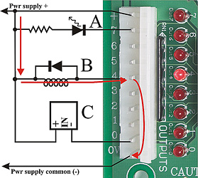
The above picture shows the output connector and three typical output devices.
The connector contains the connections for 8 outputs. It also has a positive supply connection labeled + and a common return labeled 0V.
In the picture A is an LED with a series current limiting resistor (plain LEDs must always have something in series to limit the current!).
B is a relay coil or solenoid. It has a diode across it to prevent inductive kick-backs from the coil. Although the board has suppression diodes onboard, we recommend external diodes to reduce noise problems. The diode can be a 1N4004 or similar 1A rectifier diode.
C is a solid state relay. Note the polarity labels.
The red arrow lines show the positive current path from the power supply, through the coil load and into the I/O pin, then out of the board and back to the power supply common terminal. It is absolutely essential that you provide the wire from the 0V terminal of the appropriate I/O connector back to the supply. Without that wire the current will try and find a path via the control cable back to the control board, and in the process probably burn out something.
Technical explanation: To prevent heavy switching currents from the load flowing back through the controller and causing noise problem, we have isolated the XBIO16 output ground from the controller ground with a resistor.
The (digital) outputs are implemented using the ULN2803A, a chip that contains Darlington transistors. The onboard indicator LEDs are connected directly to the output pin, and returned to the positive supply via (typically) 10K current limiting resistors.
The outputs consist of transistor switches between the output pin and 0V. When the output transistor is off, a multimeter set to DC volts connected between the output and 0V will measure a voltage slightly less than the positive supply voltage. If you set the multimeter to 200mADC, the output LED will turn on and you will get a reading of approximately V/10 milliamps, where V is the supply voltage.
Take care never to short the output pin to the positive supply voltage. If the output turns on the output chip will be instantly destroyed. This includes never doing it with a multimeter set on a current range.
There are catch diodes built into the chip. This means the board will not be damaged if you are driving relay coils, solenoid valves or other inductive loads (within the ratings of the output). We nevertheless recommend external catch diodes connected directly to the relay coil as close as possible to the relay, in order to reduce adverse effects of switching noise. The onboard diodes also mean that the load must not be connected to a supply voltage greater than the board's positive supply voltage.
If you connect the loads (for example relays) separately to the power supply or to a separate power supply, it may be possible to remove the controller's supply connection and still have power fed to the controller via the loads and the onboard protection diodes. This can produce confusing or possibly even dangerous results if the controller gets enough of this "sneak" power to run. It is safer to use the convenience + supply pin on the connector to provide positive voltage to the load.
The maximum allowable output current is 400mA steady state, with brief (100mS) peaks of 500mA allowed. There is also a limit to how much total current one ULN2803A chip can handle. This relates to the internal heating of the chip.
Let's look at 2 extreme cases:
The following table lists allowable current versus ambient temperature, when all 8 outputs are conducting the same current at once:
| Temperature | Allowable current per output |
|---|---|
| 25°C | 180mA |
| 40°C | 160mA |
| 50°C | 145mA |
| 60°C | 130mA |
| 70°C | 115mA |
The following table shows the maximum allowable currents, when concentrated in a few outputs, versus temperature
| Temp | 1st O/P | 2nd O/P | 3rd O/P | 4th O/P |
|---|---|---|---|---|
| 25°C | 400mA | 400mA | 300mA | 0 |
| 40°C | 400mA | 400mA | 150mA | 0 |
| 50°C | 400mA | 400mA | 0 | 0 |
| 60°C | 400mA | 325mA | 0 | 0 |
| 70°C | 400mA | 220mA | 0 | 0 |
Naturally there are many other possible combinations, but the above should serve as a guide.
The above figures are intended as a guide only. In any event, the absolute maximum operating temperature for the ULN2803A chip is 70°C.
If you feel like doing the actual sums, here's the procedure.
This calculation aims at a maximum internal (junction) temperature of 125°C, which is the maximum rating of the chip. There are 2 things to keep in mind with this:
Hence, an occasional excursion to, or even above, the rated temperature isn't the end of the world. However, for long life the cooler the better. The ULN2803A data sheet contains additional rating curves.
When semiconductor switches fail they are more likely to become stuck ON than OFF.