In this EasyStep you will discover the basic electrical characteristics of the EC1's digital outputs. This is a highly condensed extract from the official data sheet of the STM32F372CC chip - about 5 pages' worth of it. This applies to all digital outputs, which includes the PWM outputs.
- The processor runs off 3.3V;
- Outputs are 3.3V active high ("ON") (except outputs 0 and 1);
- Sink/source capability is symmetrical. 0.4V drop at 8mA, 1.3V at 20mA. Max rating 25mA/pin, 80mA total;
- The onboard LED outputs are available on pins 28 and 29. They are active low. Onboard they are loaded with the LED plus 220Ω (~8mA) to +3.3V.
A digital output is a pin that switches either to (close to) 0V (the negative supply) or (close to) the positive supply voltage, which in the EC1 is 3.3V nominal. We call these voltage levels "low" and "high" respectively. In the EC1 a digital output is low when it is set OFF by your program, and high when it is set ON (except outputs 0 and 1, the onboard LEDs, are the other way around). This is the opposite of the inputs. We made it this way because you are most likely to want to drive an NPN transistor off an output, in which case "active high" is the most useful.
Confused about "0V", "common", "gnd"? Click here to see some common terminology.If your background is not in the electronics field, we may confuse you a bit with the way we refer to power supply pins, grounds, "common" terminals etc. In electronics we generally quote all voltages in relation to an assumed common or reference terminal. That common terminal is often called "ground", "gnd" or "circuit ground". It may or may not actually be tied to a physical ground point, for instance mains power supply earth.
In SPLat boards we usually label the "ground" terminal "0V". On boards that are powered off an external DC power supply (which is most off-the-shelf boards), 0V is the terminal connected to the negative terminal of the power supply. Measured relative to that pin, therefore, the positive power supply pin will be 24V (or 12V or whatever the supply voltage is) positive. We then say "we have a +12V supply". All boards contain a voltage regulator chip to feed the microprocessor and/or other logic chips. In the EC1 this chip generates 3.3V nominal (many other boards use 5V). Its output voltage is said to be +3.3V, again measured relative to the 0V terminal.
Similarly, all input and output voltages are also measured relative to the 0V terminal, and will in virtually all cases be positive voltages. For example, on most SPLat models the input voltage threshold for digital inputs, and analog input and output voltages, are measured relative to 0V.
Sourcing and sinking.
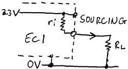
Normally, a "load" will be connected between an EC1 output and the 0V rail. A load is whatever connects to the output and gets "driven" by the output in order to do something useful. If the output is low, both ends of the load will be at the same voltage, and no current will flow. If the output goes high, positive current will flow out of the EC1 pin, through the load and into the 0V rail. This is what we call sourcing. The EC1 is sourcing current for the load.
 |
(We always think in terms of positive current flow in electronics. With all respect to electrons, that is the convention.) |
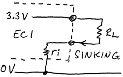
If we reverse the situation, and connect the load between the EC1 output and the positive supply rail, current will flow only when the EC1 output is low. Because the (positive) current is flowing into the EC1 pin, we say the EC1 is sinking current.
But there are limits...
The outputs of the EC1 are formed from microscopically small transistors inside the processor chip. These transistors have limits on what they can do. The main limits are these:
- The output transistors have a resistance when ON of about 65Ω (the ri in my rough sketch above). That means that if a current is flowing out of the pin, there will be some voltage dropped inside the chip, so the voltage can never get absolutely to 0V (sinking) or 3.3V (sourcing);
- A single pin is not to sink or source more than 25mA (better to stick to 20mA!);
- The total of all sink and source currents should not be more than 80mA.
.... And there are exceptions (the onboard LEDs)
Outputs 0 and 1 (pins 29 and 28 of the EC1) drive the onboard red and green LEDs. That means 3 things:
- The logic sense of these two pins is opposite to all the others. They are low when ON. That's just how we made the board - electronics designers have a predilection for active low circuits;
- We have already "used up" about 8mA of the chip's sinking capacity on each LED;
- At reset the pin will behave like 220Ω pulled up to about 2V.
Reset behaviour (advanced)
When the processor chip is fully reset, either at power on or by a hardware reset, all I/O pins go first to a high resistance state. Once the firmware gets going they are configured as outputs and set low.
If you are driving a bipolar NPN transistor through a base resistor, there should be no transient turn-on "glitch". If, however, you are driving the gate of an FET, there can be no such guarantee. If this is a problem use a 10K pulldown resistor on the gate.
On a soft reset, i.e. when the SPLat program starts, all outputs are automatically switch to the off state.
Some interesting ways to blow up your EC1
If you want to blow up your EC1, and void the warranty, here are some things you can do to the outputs:
- Connect an output, either directly or via a load, to any voltage greater than 3.3V;
- Connect an output, either directly or via a load, to any voltage more negative than 0V;
- Try to drive a relay, a motor, or any other inductive load;
- Try to drive an LED without a suitable current limiting resistor;